

- Research published in the world’s leading scientific journal, Nature
- First-ever atomic-scale identification of hierarchical moiré structures in 2D materials
- Opens new possibilities for programmable quantum material design

▲ (From left) Daesung Park (M.S. graduate, currently at Samsung Electronics), Byunghyun Kim (Integrated Master-PhD student at SNU), Prof. Changwon Park (Department of Physics, Ewha Womans University), Dr. Kunihiro Yananose (Korea Institute for Advanced Study), Prof. Young-Woo Son (IKorea Institute for Advanced Study), Prof. Hyobin Yoo (SNU Department of Materials Science and Engineering)
Seoul National University College of Engineering has announced that a joint research team led by Professor Hyobin Yoo from the Department of Materials Science and Engineering, in collaboration with Professor Young-Woo Son (Korea Institute for Advanced Study) and Professor Changwon Park (Ewha Womans University), has successfully developed a two-dimensional (2D) quantum material platform through the superposition of moiré lattices.
The research was published online on May 14 in Nature, the most prestigious journal in science and technology, under the title “Unconventional domain tessellations in moiré-of-moiré lattices.” The study was supported by the National Research Foundation of Korea’s Young Researcher Program and SRC program, the POSCO Science Fellowship from the POSCO TJ Park Foundation, and the Korea Institute for Advanced Study.
This study marks the first atomic-level identification of hierarchical structures and complex interlayer interactions resulting from the superposition of different moiré lattices in a trilayer graphene system. The work is expected to offer a promising new solid-state platform for the development of programmable quantum devices and next-generation electronic materials.
The “moiré effect” refers to a new pattern that emerges when two periodic patterns are superimposed. For example, overlapping mesh fabrics can produce wave-like patterns (see Fig. 1a), and striped shirts on TV screens may display unusual grid effects. In recent years, scientists have discovered that this visual phenomenon can also fundamentally alter the behavior of electrons in materials.
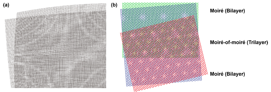
▲ Figure 1. (a) Wavy moiré pattern resulting from overlaying two layers of mesh fabric.
(b) Moiré-of-moiré pattern formed by twisting and stacking three graphene layers.
The motion and state of electrons—which are critical to the operation of electronic and quantum devices—are closely tied to how atoms are arranged and spaced within a material. In typical solids, atomic arrangements are fixed, making it difficult to control the electronic properties of materials.
However, in 2D materials such as graphene—only one atom thick—stacking two layers with a slight twist generates a new superlattice pattern called a “moiré lattice.” This creates an artificial periodicity not found in natural materials, enabling precise control of electron flow and behavior. As a result, moiré lattices are gaining attention as a platform for quantum technologies and next-generation electronics.
While past studies have primarily focused on “single moiré structures” from two stacked layers, stacking three or more layers allows different moiré lattices to form and overlap, resulting in a completely new hierarchical structure known as a “moiré-of-moiré lattice” (see Fig. 1b). Because each moiré period can be independently tuned, this configuration greatly enhances the degrees of freedom in controlling electronic states.
Despite its potential, the mechanisms behind these multi-moiré structures remain poorly understood. Investigating how such complex structures form and how interlayer interactions govern their behavior is essential for designing more sophisticated electronic systems in the future.
To explore this, the joint research team stacked three layers of graphene with carefully controlled twist angles, creating overlapping moiré lattices (see Fig. 1b). Using high-resolution transmission electron microscopy (TEM), they directly observed novel lattice patterns that spontaneously emerged from atomic rearrangements, including previously unreported triangular, kagome*, and hexagram motifs (see Figs. 2a and 2b).
*Kagome: A lattice structure made of interlaced triangles and hexagons.
These patterns emerged as atoms self-organized into energetically favorable configurations behavior that nearest-layer interactions alone cannot explain. The team revealed that weak yet crucial interactions also occur between non-neighboring layers, playing a significant role in determining the overall structure.
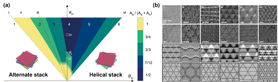
▲ Figure 2. (a) Phase diagram of domain lattice as a function of twist angle. (b) Spontaneously formed domain lattice structure.
As a result of these intricate interlayer interactions, the resulting hierarchical lattice patterns and distinctive physical properties manifest exclusively in trilayer and thicker multilayer systems. To elucidate these structures, the team combined transmission electron microscopy measurements with computational simulations and report a “structural phase diagram” that maps how various domain lattices emerge as a function of twist angle(see Figs. 2a and 2b). This phase diagram is expected to serve as a valuable guide for future design of quantum materials using multi-moiré lattices.
This research demonstrates that hierarchical atomic arrangements and electronic states can be precisely designed even in complex, multi-moiré systems—going beyond the limitations of single moiré structures. The ability to control two moiré periodicities independently offers greater freedom in designing electronic properties.
Moreover, the team successfully revealed new quantum mechanical phenomena in hierarchical moiré structures and devised novel methodologies to elucidate their behavior from a materials science and physics perspective. These advances are expected to enable more sophisticated material designs for future 2D quantum material platforms and provide a foundation for developing new types of electronic and computational devices.
Professor Hyobin Yoo, who led the study, stated, “This research shows that moiré structures are more than just visual patterns—they can serve as powerful tools for engineering atomic interactions and electronic states. The hierarchical lattice formation and long-range interlayer interactions seen in moiré-of-moiré lattices open up entirely new pathways for material design.”
He added, “In the future, we expect this research to lead to the development of ‘programmable materials’ whose electronic properties and lattice structures can be actively tuned using external stimuli such as electric fields—paving the way for applications in next-generation electronics and quantum technologies.”
Co-first author Daesung Park conducted research on moiré lattices in twisted van der Waals (vdW) materials using TEM during his master’s studies. He is now working at Samsung Electronics as a Process Architecture (PA) engineer, where he focuses on designing and developing advanced semiconductor manufacturing processes to improve performance and cost efficiency.
[Reference Materials]
- Paper/Journal : ‘Unconventional domain tessellations in moiré-of-moiré lattices‘, Nature
- DOI : https://doi.org/10.1038/s41586-025-08932-0
[Contact Infromation]
Professor Hyobin Yoo, Materials & Device Analysis Lab, Department of Materials Science and Engineering, Seoul National University / +82-2-880-1550 / hyobinyoo@snu.ac.kr