- Achieves a 0.7mm-thick lens system using nano-optical device ‘metasurfaces’
- Published in the prestigious international journal Science Advances.

▲ Youngjin Kim (left) and Taewon Choi (right), researchers at Seoul National University’s Optical Engineering and Quantum Electronics Laboratory, Department of Electrical and Computer Engineering.
Seoul National University College of Engineering announced that researchers from the Department of Electrical and Computer Engineering’s Optical Engineering and Quantum Electronics Laboratory have developed an optical design technology that dramatically reduces the volume of cameras with a folded lens system utilizing “metasurfaces,” a next-generation nano-optical device.
By arranging metasurfaces on the glass substrate so that light can be reflected and moved around in the glass substrate in a folded manner, the researchers have realized a lens system with a thickness of 0.7mm, which is much thinner than existing refractive lens systems. The research, which was supported by the Samsung Future Technology Development Program and the Institute of Information & communications Technology Planning & Evaluation (IITP), was published on Oct. 30 in the prestigious international journal Science Advances.
Traditional cameras are designed to stack multiple glass lenses to refract light when capturing images. While this structure provided excellent high-quality images, the thickness of each lens and the wide spacing between lenses increased the overall bulk of the camera, making it difficult to apply to devices that require ultra-compact cameras, such as virtual and augmented reality (VR-AR) devices, smartphones, endoscopes, drones, and more.
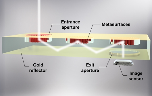
To address this limitation, The researchers have developed an ultra-thin camera system that reduces the thickness of a conventional lens system by less than half, using a new lens module design that incorporates metasurfaces. Metasurfaces, which are being touted as the next generation of nano-optical devices, have the ability to precisely control the three properties of light - intensity, phase, and polarization - on a pixel-by-pixel basis. This is because the nanostructures that make up a metasurface are arranged in periods of a few hundred nanometers (nm), which is shorter than the wavelength of light. According to the team, by designing a metasurface optimized for a specific wavelength (852 nm) and arranging multiple sheets horizontally on a glass substrate, light can be reflected multiple times inside the substrate, thereby space-efficiently securing the light paths in a folded manner. The team presented a structure for a miniaturized camera that captures images with a system of thin, folded lens module that adjust the path of light.
The system not only overcomes the physical limitations of thick conventional lens modules, but also delivers superior image quality. This is because it provides a 10-degree field of view within a very small system footprint of 0.7 millimeters thick, and delivers high-resolution images close to the diffraction limit at an aperture of f/4 and a wavelength of 852 nm. Thanks to these strong competitive advantages, the miniaturized camera technology developed by the researchers is expected to be widely applied in various advanced optical device industries such as VR-AR devices, smartphones, medical endoscopes, and miniaturized drones.
“This research is significant in that it provides a creative breakthrough to innovatively reduce the thickness of cameras by introducing nano-optical devices,” said Youngjin Kim, first author of the paper. ”We will continue our research to lead the innovation of thin and light cameras with metasurfaces that combine excellent performance and industrial benefits thanks to their nanometer-scale light tuning freedom and fabrication through semiconductor processes.”
“Our research focuses on efficiently utilizing the lens space by using metasurfaces,” said Taewon Choi, co-first author of the study. ”The folded lens system is very thin, unlike conventional systems that are thick due to the combination of multiple lenses, so it will play an important role in the virtual and augmented reality industry, where device miniaturization and lightweight are essential.”
The Optical Engineering and Quantum Electronics Laboratory, where the research was conducted, is currently led by Prof. Yoonchan Jeong following the passing of Prof. Byoungho Lee in November 2022. The lab continues its active research in 3D displays, holography, and metasurfaces. Researcher Young Jin Kim will continue his research on overcoming the limitations of imaging devices such as cameras by utilizing metasurfaces. Taewon Choi plans to continue his research on the application of metasurfaces in VR-AR devices, camera sensors, image sensors, and other related industries.

▲ A schematic of a next-generation ultra-thin camera that utilizes metasurfaces, a nano-optical device, to secure light paths: By aligning metasurfaces horizontally on a glass substrate, light reflects multiple times within the substrate, securing space-efficient light paths in a folded manner.

▲ (Left) Comparison of thickness between a conventional smartphone lens module and the developed metasurface lens module. (Center) Microscopic image of the metasurface nanofabrication. (Right) Image of the nanostructures composing the metasurface.

