Since the successful isolation of graphene from bulk graphite, remarkable properties of graphene have attracted many scientists to the brand-new research field of 2D materials. However, despite excellent carrier mobility of graphene, direct application of graphene to field-effect transistors is severely hindered due to its gapless band structure. Alternatively, semiconducting transition metal dichalcogenides (TMDCs) have been focused intensively over the last decade. However, wide bandgap 2D materials with > 3 eV have been required for UV-related optoelectronic devices, power electronics, and dielectric layers.
One of promising candidates is transition metal oxides (TMOs), which has large bandgap, structural diversity, and tunable physical/chemical characteristics. Nevertheless, the scalable growth of atomically-thin TMOs remains challenging until now since it is very prone to the lattice-mismatch strain and strong substrate clamping during growth.
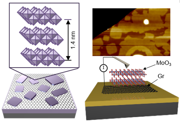
Recently, the research team led by Prof. Gwan-Hyung Lee of Seoul National University overcame the issue by employing the van der Waals (vdW) epitaxial growth method. The research team reported a novel method for scalable growth of orthorhombic molybdenum oxide(α-MoO3) nanosheets on the graphene substrate. An important question in this work is what the effect of thickness on the electrical and physical properties is. To figure out this, comprehensive atomic force microscopy (AFM) studies were performed to explore structural and electrical properties of MoO3 layers with various thickness. Interestingly, AFM study revealed that MoO3 nanosheets retain bulk-like structural and electrical properties even when MoO3 nanosheets are thicker than 2 ~ 3 layers (1.4 ~ 2.1 nm in thickness). Especially, the thickness-sensitivity of friction is very small compared to other hexagonal 2D materials. This intriguing result is attributed to the doubled octahedral planes of monolayer MoO3 with exceptionally small interatomic separation. Additionally, work function and dielectric constant are also thickness-independent, along with invariant electronic band structure regardless of the thickness. Besides, the team showed that MoO3 nanosheets obtain large current gap and high dielectric constant, emphasizing that MoO3 can be used as a promising 2D dielectric materials.
The research, " Thickness-insensitive properties of α-MoO3 nanosheets by weak interlayer coupling” was published in November, 2019, in the Nano Letters.
In addition to the team leader, Prof. Gwan-Hyoung Lee, Dr. Jong Hun Kim, and Ph.D. candidate Hangyel Kim are affiliated with Seoul National University. Other authors, Dr. Changbae Hyun and Dr. Kyuwook Lhm are affiliated with Pohang University of Science and Technology. Prof. Jatis Kumar Dash is a professor of SRM University-AP.
This work was supported by the Basic Science Research Program through the National Research Foundation of Korea (NRF) funded by the Ministry of Science, ICT & Future Planning (NRF-2017R1A2B2006568, 2018M3D1A1058794), and the Korea Institute of Energy Technology Evaluation and Planning (KETEP) and the Ministry of Trade, Industry & Energy(MOTIE) of the Republic of Korea (No. 20173010013340). C. H. acknowledge supports by the Korea Research Fellowship Program through NRF funded by the Ministry of Science, ICT, and Future Planning (2016H1D3A1938061 and NRF-2016R1D1A1B01011181). K.I. was supported by NRF (NRF-2018R1D1A1B07043155) through the Ministry of Science, ICT, and Future Planning, Korea. Experiments at PLS-II were supported by MSIP-R. O.,Korea

Graphic showing a crystal structure of MoO3 nanosheet grown on hexagonal graphite (left). To characterize physical and electrical properties of MoO3, atomic force microscopy was conducted (right).

