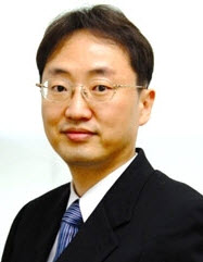
Professor HONG Yongtaek, Department of Electrical and Computer Engineering
A team led by Professors Yongtaek Hong (Department of Electrical and Computer Engineering) and Zhenan BAO (Department of Chemical Engineering, Stanford University) has developed a novel technique which enables large area formations of organic semiconductors (OSCs). Practical applications of organic electronics require patterned and precisely registered OSC films with uniform electrical properties over a large area, which remained a challenge. The team came up with “controlled OSC nucleation and extension for circuits” (CONNECT), which uses differential surface energy and solution shearing to simultaneously generate self-patterned and self-registered OSC film with low variability in electrical properties over a large area. The team succeeded in fabricating transistor density as high as 840 dpi, with a yield of 99%.
- The details of this development were published online in PNAS (Proceedings of the National Academy of Sciences) on April 20.
- Professors HONG Yongtaek's lab: http://axel.snu.ac.kr/xe/
- SNU Department of Electrical and Computer Engineering: http://ee.snu.ac.kr/en
Summary by LEE Hee Un, SNU English Editor, gurume0221@snu.ac.kr
Proofread by Melora Brett Briana Johnson, morningcalm2@gmail.com

